What Is SMT? Components, Process and Assembly Decisions
MOZPCB Editorial Team (PCB manufacturing guides) · Updated 2026/11/13
SMT stands for surface-mount technology: an assembly method in which component terminations attach to lands on a PCB surface. A common production route prints solder paste onto the board, places components on that paste and reflows the solder to form joints.
SMD means surface-mount device, the component itself. PCBA means printed circuit board assembly, the populated board produced by SMT, through-hole assembly or both. Keeping these terms separate helps specify whether an order covers bare boards, components, assembly operations or a tested product.
SMT, SMD, THT and PCBA compared
A component package determines how its connections meet the board. The selected assembly process must match those connections; a BOM alone does not describe every manufacturing operation.
| Term | Meaning | Example use in an order |
|---|---|---|
| SMT | Surface-mount assembly technology | Print, place and reflow the specified surface-mount parts |
| SMD | A device designed for surface mounting | An exact resistor, IC or connector manufacturer part number |
| THT | Through-hole technology using leads or pins through board holes | Insert and solder selected connectors after the SMT operations |
| PCBA | The populated circuit-board assembly | Deliver the specified variant with agreed inspection/programming/test |
Which component packages use SMT?
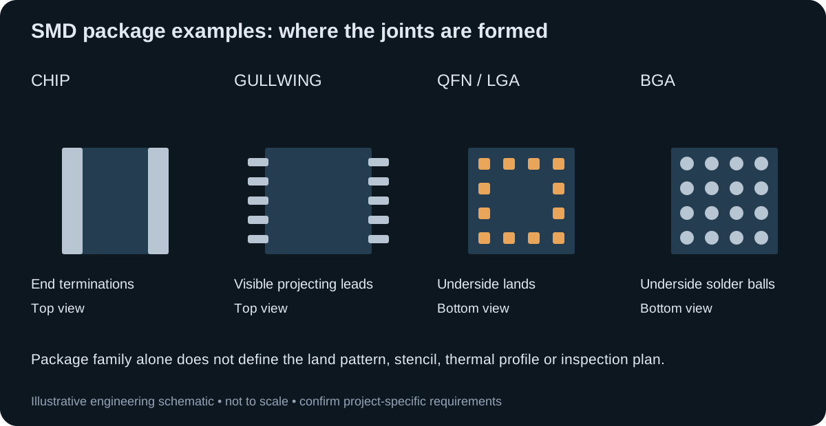
SMT includes chip resistors and capacitors, leaded ICs, bottom-terminated packages, BGAs and many connectors. Some joints are visible at the package perimeter; others lie underneath the body. That difference influences inspection and rework access.
Do not identify a chip component solely by a size code. Imperial and metric naming systems can use similar numbers for different dimensions. Provide the manufacturer part number, package drawing and CAD footprint identity, especially when substituting a BOM item.
| Package family | Connection location | Assembly question |
|---|---|---|
| Chip passive | Terminations at the ends | Are pad geometry, paste and thermal balance suitable for the actual size? |
| Gull-wing IC | Leads extend beyond the package | Are pitch, lead condition, polarity and visible joint access addressed? |
| QFN / LGA and similar | Terminations mainly underneath the package | Are exposed-pad paste, via treatment and hidden-joint inspection defined? |
| BGA | Array of solder balls beneath the body | Are land pattern, escape vias, thermal process and X-ray/test scope agreed? |
| Surface-mount connector | Surface lands plus possible locating or retention features | Are mating loads, anchors, overhang and reflow limits suitable? |
How does an SMT line turn paste and parts into joints?
Paste printing deposits solder paste through stencil apertures. The copper land pattern and stencil design are related but distinct; changing one globally to compensate for the other can create defects elsewhere. Board support and fiducial alignment help place the deposit where the program expects it.
Placement uses a component library, feeder assignments, coordinates, side and rotation data. A component centered on the correct location may still be wrong if the package rotation or pin-one interpretation is incorrect. Verify the released BOM, CPL and assembly drawing together.
Reflow heats the assembly through a profile selected for paste, components and board construction, then cools it to form the joints. The profile is not just an oven setpoint: the assembly must reach suitable conditions without exceeding applicable material limits. No single peak temperature or side sequence covers every BOM.
Inspection can occur at several stages, such as paste inspection before placement and optical or X-ray inspection after soldering. The full PCB assembly process guide covers incoming checks, mixed-technology sequencing and lot release.
When does SMT make sense, and when is a mixed build needed?
SMT supports dense layouts and automated placement for many package families. It can also place components on both sides of a board. Those possibilities introduce decisions about handling, thermal exposure, fixture access and inspection rather than guaranteeing a lower price for every design.
A product may retain through-hole or press-fit connectors for its mechanical interface while using SMT for most circuitry. Review the exact connector rating and retention design; surface-mount does not automatically mean mechanically weak, and through-hole does not automatically prove system reliability.
Use SMT versus through-hole assembly for the detailed comparison. This page establishes the terminology and preparation questions; the comparison guide addresses technology trade-offs.
What can inspection prove about an SMT assembly?
AOI can evaluate accessible placement, orientation and solder features within its programmed coverage. X-ray can provide evidence about hidden solder geometry. Neither automatically establishes correct component electrical values, firmware behavior or product performance.
An SMT assembly can be visually acceptable and still fail a functional test. Define electrical access, fixture/software ownership and measurable operating limits if the order needs functional verification. The PCB versus PCBA guide separates these purchasing and testing responsibilities.
What changes SMT cost and lead time?
BOM availability, packaging format, setup count, assembled sides, package mix, stencil/tooling and test time all influence the quote. A low component count with difficult hidden joints and a long functional test may require more work than a larger count of familiar parts.
Separate one-time setup from recurring assembly and component procurement. For comparisons, keep quantity, revisions, material responsibility and test scope fixed; the assembly cost guide develops this model without treating a teaching estimate as a real quote.
The release packet for an SMT quote
Send the fabrication package and board revision, BOM with manufacturer part numbers, centroid/CPL with units/origin/side/rotation, assembly drawing, DNP list, approved alternates and intended panel. Specify who supplies boards and components, and provide programming/test instructions if needed.
For new package families, attach the manufacturer land pattern and soldering guidance. Flag via-in-pad lands, unusual solder-mask boundaries, mixed technologies and any inaccessible joints. The assembler should confirm library interpretation and tooling before the first lot.
Use SMT assembly services to request a review tied to that packet. Agree the first-article approval point, required records and who can approve changes before releasing the balance of the order.
Frequently asked questions
Is SMT the same as SMD?
Does SMT mean the board has no holes?
Can SMT components be assembled on both sides?
Does an SMT quote include components?
Is X-ray inspection the same as functional testing?
Sources
- PCB Basics — surface-mount, paste and reflow terminology — SparkFun Electronics
Related articles
- PCB Assembly2026/07/08 · 5 min
SMT vs Through-Hole Assembly: Process and Cost Differences
When surface-mount wins, when through-hole still matters, and how mixed-technology boards sequence SMT, wave, and selective solder without yield surprises.
Read article - PCB Assembly2026/11/13 · 6 min
PCB Fiducial Marks: Global and Local Alignment Guidelines
A practical fiducial release checklist connecting optical targets, panel rails, mask data and placement coordinates to the assembler’s equipment requirements.
Read article - PCB Assembly2026/11/02 · 7 min
PCB Assembly Process: BOM Review, Placement, Reflow and Test
Understand the SMT and through-hole assembly flow, its inspection gates and the files needed to define a build that can actually be accepted.
Read article - PCB Assembly2026/10/13 · 4 min
Turnkey PCBA RFQ Checklist
Everything a turnkey PCB assembly quote request needs—fabrication data, BOM and sourcing notes, assembly instructions, and test requirements—in one reviewable package.
Read article