High-Frequency PCB Manufacturer
MOZPCB is a high-frequency PCB manufacturer for hardware teams that have outgrown FR-4. We fabricate Rogers, PTFE, and hybrid boards with dielectric control and impedance verification RF designs depend on.
Service overview
Choosing a high-frequency PCB manufacturer is a materials-and-process decision, not a catalog checkbox. Above roughly 1 GHz, standard FR-4 Dk drift and loss start showing up in filters, antennas, and long channels. MOZPCB fabricates those boards on Rogers, PTFE, and hybrid stackups with disciplined etch control, matched lamination profiles, and impedance coupons your RF team can measure.
High-frequency PCBs are built on laminates engineered for stable dielectric constant (Dk) and low loss tangent (Df) across frequency and temperature—materials like Rogers RO4350B and RO4003C, PTFE-based laminates, and other low-loss systems. Getting RF performance right is less about exotic processes and more about disciplined material handling: controlled etching for trace geometry, correct lamination profiles, and impedance verification against your tables.
Many RF products do not need expensive laminate on every layer. Hybrid stackups place a Rogers or PTFE layer where the RF signals live and standard FR-4 in the digital and power sections, cutting material cost significantly. We review your stackup and recommend where hybrid construction makes sense before quoting.
Every high-frequency quote includes an engineering review of Dk assumptions, copper roughness implications, and impedance tolerance expectations, because a board that meets the drawing but misses the modeled Dk still fails in the tuning lab. Typical laminate and impedance windows sit on the PCB capabilities table; thermal-only designs that do not need RF laminates usually belong on metal-core PCB instead.
What we offer
- Rogers RO4350B and RO4003C builds—the workhorse laminates for RF below ~40 GHz
- PTFE and ceramic-filled PTFE laminates for the most demanding microwave designs
- Hybrid Rogers + FR-4 stackups that keep low-loss material only where RF routing needs it
- Controlled impedance with documented targets, tolerances, and coupon testing
- Edge plating, cavity structures, and copper coin insertion subject to design review
- Low-profile and reverse-treated copper foils where insertion loss budgets are tight
- Surface finishes suited to RF: immersion silver, ENIG, and ENEPIG per your loss budget
- RF assembly including connector launch soldering and shield fence placement
Technical capabilities
- Material systems: Rogers RO4000 series, PTFE-based laminates, and hybrid constructions (availability confirmed per project)
- Dielectric constant control per laminate datasheet with lot traceability
- Impedance control typically to ±7%, tighter tolerances reviewed case by case
- Hybrid lamination of dissimilar materials with matched press profiles
- Line width and spacing suited to microstrip and grounded coplanar waveguide geometries
- Back-drilling to shorten via stubs on thicker high-speed builds
- Test coupons and TDR reports delivered with impedance-controlled orders
| Material | Approx. Dk | Df (typical) | When teams pick it |
|---|---|---|---|
| FR-4 (standard) | ~4.2–4.8 | ~0.02 | Below ~1 GHz, short runs, cost-first digital |
| Rogers RO4003C | ~3.38 | ~0.0027 | Microwave / RF where flame rating is not required |
| Rogers RO4350B | ~3.48 | ~0.0037 | Commercial RF that needs UL 94 V-0 |
| PTFE / ceramic PTFE | ~2.2–3.0 | Very low | Highest-frequency / lowest-loss channels |
| Hybrid Rogers + FR-4 | Mixed | RF layer only | RF on one or two layers; digital/power on FR-4 |
Common applications
- 5G and LTE antennas, small cells, and RF front-end modules
- Radar sensors for automotive, industrial, and security applications (24/77 GHz reviewed per design)
- Satellite communication and GPS/GNSS receivers
- RF power amplifiers, filters, couplers, and low-noise amplifier boards
- High-speed digital backplanes where loss budgets rule out standard FR-4
How the process works
- 01
Requirements intake
Share Gerber, BOM, drawings, quantities, and any reliability or compliance notes.
- 02
Technical alignment
We confirm materials, finishes, assembly flow, and test expectations with you.
- 03
Production & inspection
Manufacturing and assembly follow the agreed traveler with documented checks.
- 04
Delivery
Packing, labeling, and shipment according to your logistics instructions.
In our factory
-
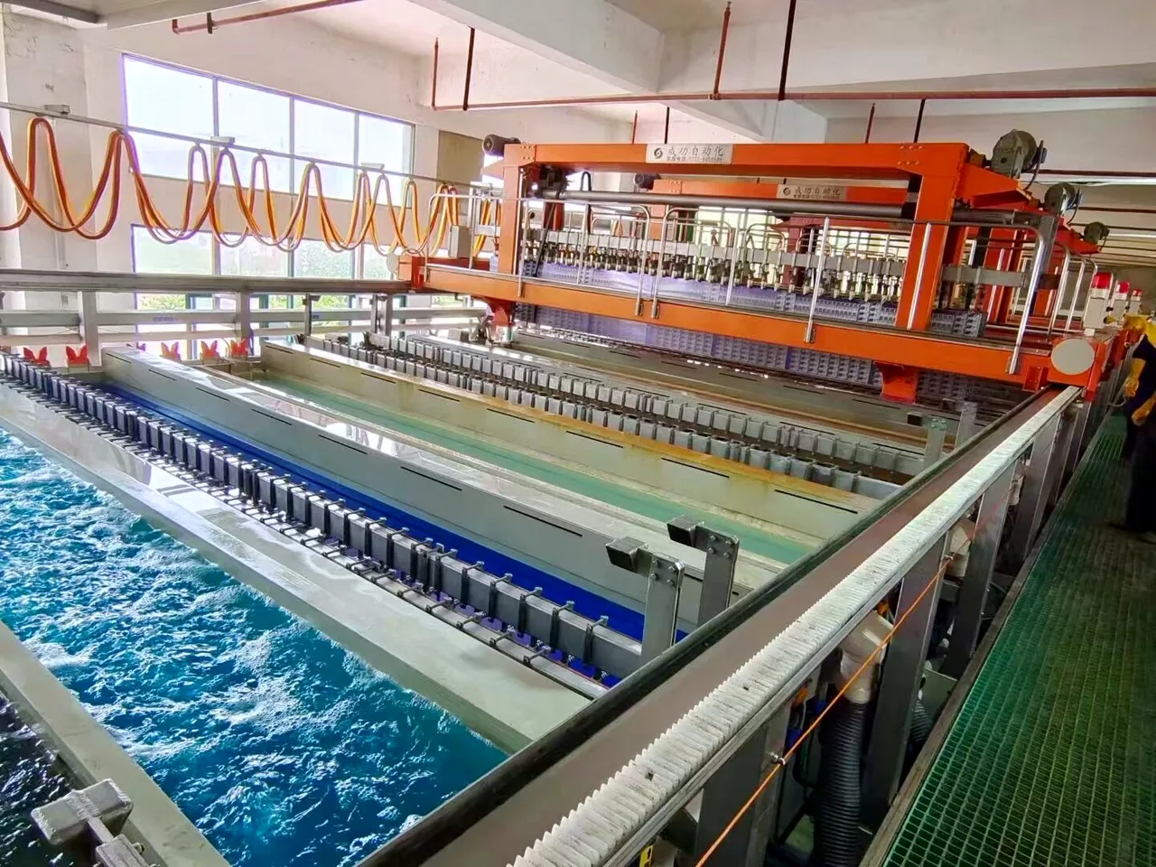
Plating line -
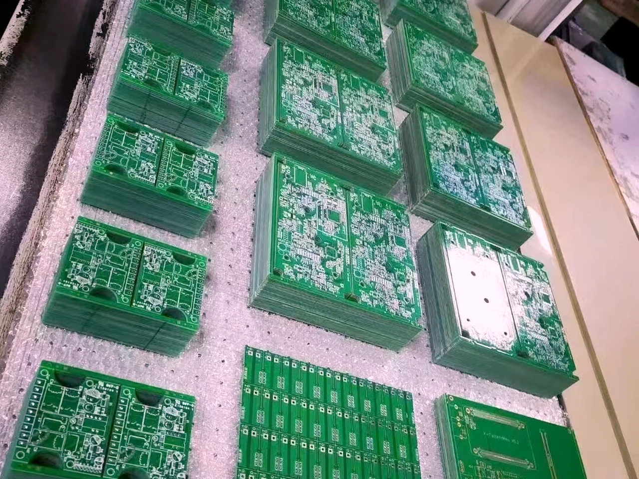
Panelized boards -
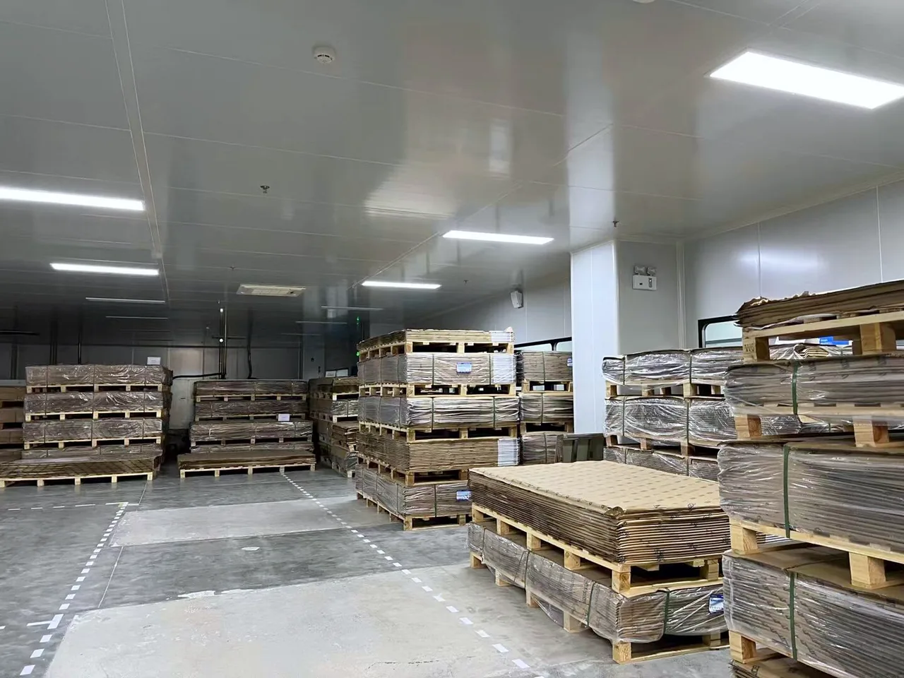
Laminate store
Related services
Related guides
FAQ
When should I move from FR-4 to a high-frequency laminate?
Rogers RO4350B vs RO4003C—which should I choose?
What is a hybrid stackup and how much does it save?
How tight can impedance tolerance be on high-frequency boards?
Does copper roughness really matter for my design?
What should I send a high-frequency PCB manufacturer in the first RFQ?
Get started
Ready for the next step?
Send your project files and requirements. We will review stackup, assembly, and test needs, then respond with a clear quotation path.