Via-in-Pad PCB Guide: Filled, Capped, Tented and HDI Vias
MOZPCB Editorial Team (PCB manufacturing guides) · Updated 2026/11/02
Explore design and stackup guides →
A via-in-pad is a via placed within a component solder land, commonly to shorten escape routing or connect a thermal pad to internal copper. An untreated open hole may draw solder away from the joint, so the required via treatment must be part of the fabrication drawing.
There is no universal BGA pitch at which every design requires via-in-pad. Package geometry, pad size, line/space rules, layer count and routing direction determine whether a conventional dog-bone fanout, blind microvia or filled-and-capped via is appropriate.
Dog-bone fanout versus via-in-pad
Dog-bone fanout connects a pad to a nearby via with a short trace. It can avoid a hole directly inside the solder joint but consumes routing area. Via-in-pad can release that area, especially in dense packages, while adding process and inspection requirements.
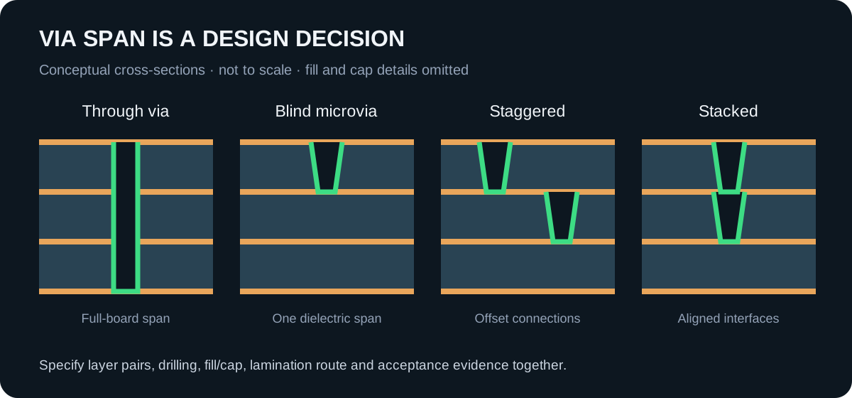
A through via in a pad still spans the board and can create an electrical stub. A blind microvia connects selected nearby layers and changes the manufacturing route. Review the signal path, reference-plane transition and available escape channels before choosing solely by pad pitch.
Tented, plugged, filled and capped are not synonyms
Use unambiguous process notes and the applicable via-protection specification when needed. A phrase such as “all vias plugged” is insufficient for a critical BGA land.
| Treatment | What it generally means | What not to assume |
|---|---|---|
| Tented | Mask covers one or both openings | Not a solid fill or planar copper pad |
| Plugged | Material obstructs part of an opening/hole | Not necessarily full-depth filling |
| Filled | Specified material occupies the via | Does not by itself define a copper cap |
| Filled and capped | Filled/planarized via with specified copper cap | Fill material, cap integrity and planarity still need limits |
| Copper-filled microvia | Microvia filled by a qualified plating process | Not equivalent to resin-filled through via |
Choosing fill material and a surface suitable for soldering
Resin-filled and copper-capped mechanically drilled vias and copper-filled microvias can both appear in dense designs, but their process routes differ. Conductive and nonconductive fills also have different properties; the word “conductive” does not by itself prove a better thermal path or more reliable joint.
Specify the hole type and span, fill material or approved process, cap requirement, planarity and acceptable void criteria. The assembler needs a land geometry that supports the paste volume and joint design. Share the component land pattern and stencil assumptions when the package is sensitive to solder loss or surface depression.
HDI stackup and reliability review
Stacked microvias place connections above one another; staggered microvias offset them between build-up layers. Either route must be evaluated against available area, registration, plating, interfaces and the product reliability requirement. More build-up layers mean more opportunities for process variation.
Ask for the proposed lamination and drilling sequence and the evidence required for qualification or lot acceptance. Cross-sections, continuity tests and thermal-stress evaluations answer different questions. A visually plausible cross-section is not proof of lifetime reliability. Coordinate the HDI design guide with the actual mission profile.
Cost drivers and RFQ requirements
Cost depends on via count and type, fill and planarization, copper capping, sequential lamination, inspection and yield—not simply whether the drawing says HDI. Where routing allows, compare a simpler through-via or staggered architecture before accepting a more complex build.
Send a via table naming each group, start/end layers, drill or laser diameter, land sizes, fill/cap treatment and related component pads. Include board thickness, copper, stackup, quantity and acceptance requirements. For thermal pad vias, discuss solder-paste aperture and void requirements with assembly instead of importing a signal-BGA rule.
Frequently asked questions
Must every via-in-pad be filled and capped?
Is via-in-pad the same as HDI?
Can solder mask replace a copper cap?
Are stacked microvias always better than staggered vias?
Related articles
- PCB Design2026/11/02 · 4 min
Standard PCB Thickness: Sizes, Tolerances and Stackup Choices
1.6 mm is common, not mandatory. Choose finished thickness from mechanical fit, stackup and the tolerance your assembly actually needs.
Read article - PCB Design2026/11/02 · 4 min
1 oz vs 2 oz Copper PCB: Thickness, Current and Design Trade-offs
Copper weight is mass per area, not a current rating. Understand what thicker copper changes before putting 2 oz on every layer.
Read article - PCB Design2026/11/02 · 4 min
What Is a PCB? Layers, Materials, Types and How to Order
A beginner-friendly explanation of the printed circuit board, with practical distinctions that matter when moving from a design to a manufacturing quote.
Read article - PCB Manufacturing2026/11/02 · 4 min
PCB vs PCBA: Differences, Files, Cost and Ordering Scope
Understand what you receive from a bare-board order versus an assembled-board order, and which files and tests belong in each quote.
Read article