What Is a PCB? Layers, Materials, Types and How to Order
MOZPCB Editorial Team (PCB manufacturing guides) · Updated 2026/11/02
Explore design and stackup guides →
A PCB, or printed circuit board, is a structure that supports electronic components and connects them through patterned copper conductors. Instead of wiring every connection individually, a designer defines traces, planes, pads and vias on one or more conductive layers separated by insulating material.
The word “printed” is historical: many modern rigid boards are made with imaging, etching, lamination and plating rather than printing ordinary conductive ink. The useful starting point is to understand what each layer and feature does, then choose a construction that fits the product.
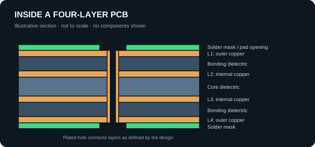
The main parts of a PCB
A board’s green surface is typically solder mask, not the insulating core itself. A copper pad may appear gold or silver because a surface finish protects the exposed copper before assembly.
| Part | Role |
|---|---|
| Dielectric / substrate | Insulates conductors and provides mechanical structure |
| Copper traces and planes | Carry signals, power and return currents |
| Pads | Provide connection lands for components or contacts |
| Vias and plated holes | Connect copper on different layers |
| Solder mask | Covers selected copper and defines exposed areas |
| Surface finish | Protects exposed lands and supports connection/soldering |
| Legend / silkscreen | Labels components, polarity and board identity |
Single-sided, double-sided and multilayer boards
A single-sided board has one copper circuit layer; a double-sided board has copper on both sides, often interconnected through plated holes. A multilayer board includes internal copper layers as well. Layer count refers to conductive layers, not the number of visible colors or the number of component sides.
More layers can make routing and return-path control easier, but they add stackup decisions and cost. An internal plane may distribute power or provide a signal reference. Choose layer count from routing density, noise, power and mechanical requirements rather than assuming that more layers always means a better board.
Rigid, flex, rigid-flex and specialty materials
Rigid FR-4 boards are common for general electronics. FR-4 describes a family of glass-reinforced epoxy material systems, not one universal electrical or thermal specification. High-frequency or demanding thermal applications may require a different laminate or construction.
A flex PCB uses a flexible dielectric structure; rigid-flex combines rigid regions with flex sections. Metal-core constructions provide a different thermal path for some applications. Material selection must consider temperature, dielectric properties, mechanical use, assembly and availability—not just a familiar material name.
From schematic to bare board and assembled product
A schematic defines electrical intent. Layout assigns component locations and turns connections into copper geometry within a stackup. Manufacturing output then defines copper, mask, drills, outline and fabrication requirements. The fabrication process produces the bare board.
Assembly adds components and solder joints, producing a PCBA. Programming, functional testing, enclosure integration and product approval are additional activities when required. The PCB versus PCBA comparison explains how to keep those scopes clear in a quote.
What a first PCB order needs
At minimum, prepare the manufacturing files, drill data, outline, layer order, material requirement, finished thickness, copper, finish, quantity and revision. Include impedance, via treatment, special dimensions or inspection requirements when they apply. A screenshot of the layout is useful for discussion but is not a manufacturing package.
For an assembled prototype, also supply a BOM with manufacturer part numbers, placement data, assembly drawing, polarity and DNP notes. Ask the supplier to resolve missing requirements before tooling. Use the Gerber preparation checklist and start with a prototype sized to answer the design questions you need to test.
Frequently asked questions
What does PCB stand for?
Is a motherboard a PCB?
Why are most PCBs green?
Can a PCB work without components?
Related articles
- PCB Design2026/11/02 · 4 min
Standard PCB Thickness: Sizes, Tolerances and Stackup Choices
1.6 mm is common, not mandatory. Choose finished thickness from mechanical fit, stackup and the tolerance your assembly actually needs.
Read article - PCB Design2026/11/02 · 4 min
1 oz vs 2 oz Copper PCB: Thickness, Current and Design Trade-offs
Copper weight is mass per area, not a current rating. Understand what thicker copper changes before putting 2 oz on every layer.
Read article - PCB Design2026/11/02 · 4 min
Via-in-Pad PCB Guide: Filled, Capped, Tented and HDI Vias
Via-in-pad can save routing space, but a pad location alone does not define the fill, cap, planarity or reliability requirements.
Read article - PCB Manufacturing2026/11/02 · 4 min
PCB vs PCBA: Differences, Files, Cost and Ordering Scope
Understand what you receive from a bare-board order versus an assembled-board order, and which files and tests belong in each quote.
Read article