PCB Manufacturing Process: From Gerber to Finished Board
MOZPCB Editorial Team (PCB manufacturing guides) · Updated 2026/11/02
Explore manufacturing and assembly guides →
A PCB manufacturing process turns a defined set of circuit layers, holes, materials, and mechanical features into a bare board that can be assembled. The exact route depends on the construction: a simple two-layer rigid board does not use the same sequence as HDI, rigid-flex, or a hybrid RF stackup. The flow below describes a common subtractive rigid multilayer build; a fabricator may use a different sequence or process for a particular design.
Before production starts, the fabricator reviews the fabrication data and resolves mismatches between Gerbers, drill files, stackup, dimensions, impedance notes, finish, and the assembly plan. That review is where a clear package prevents avoidable quote assumptions and production holds.
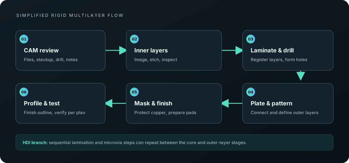
1. CAM review turns design files into a build plan
CAM engineering checks that each copper, solder-mask, silkscreen, drill, and outline file has a clear purpose and matches the layer map. The team also reviews the stackup, board dimensions, hole types, surface finish, controlled-impedance requirements, and special notes such as edge plating or via-in-pad. If the drawing and data disagree, the open point should be resolved before tooling.
Send a consistent layer map, NC drill files with plated versus non-plated holes identified, board outline, stackup, and fabrication notes. The Gerber preparation checklist explains how to package these files for review.
| Input | What the fabricator needs to understand |
|---|---|
| Layer map and stackup | Layer order, dielectric targets, finished thickness, and copper weight |
| Drill data | Hole sizes, plated/non-plated intent, slots, and via spans |
| Fabrication notes | Finish, impedance targets, special processes, and acceptance requirements |
2. Inner-layer imaging and etching form the circuit pattern
For a multilayer rigid board, copper-clad core material is prepared and coated with photoresist. Artwork is aligned and imaged onto the resist; after development, exposed copper is etched away to leave the intended traces, pads, and planes. Optical inspection can compare the patterned layer with its digital data before the layers are stacked.
Copper balance, spacing, and registration affect what can be built reliably. These details should be reviewed against the selected material and approved capability range instead of assuming one line-width limit applies to every layer and copper weight.
3. Lamination and drilling join the layers
The patterned cores are aligned with prepreg and copper foil, then bonded under heat and pressure into a multilayer panel. Registration targets and the stackup determine how the internal layers line up with one another. After lamination, mechanical drills create through-holes; laser drilling may be used for microvias on an HDI design.
A standard through-hole board and an HDI board can differ substantially here. Sequential lamination and microvia formation add cycles, so the layer map and via architecture must make clear which holes connect which layers. See the HDI PCB design guide before specifying blind, buried, or stacked microvias.
4. Copper plating and outer-layer patterning complete connections
For plated through-holes, the drilled panel is prepared so copper can be deposited on the hole walls and connect the copper layers. The outer copper layers are then patterned and etched to create the final surface traces and pads. Depending on the build, inspection may check registration, plated features, and the outer-layer artwork against the manufacturing data.
If the board requires controlled impedance, the actual dielectric construction, copper, trace geometry, and reference planes must match the approved stackup. Specify the controlled structures and coupon requirements in the fabrication package; a nominal “50 ohm” note by itself does not define the complete test plan.
5. Solder mask, surface finish, profiling, and test prepare the bare board
Solder mask is applied and opened where pads must remain exposed. Silkscreen may then identify components or board information. The selected surface finish protects exposed copper and supports the planned assembly process. Board outlines, slots, and scored features are routed or profiled to the approved mechanical drawing.
Electrical testing commonly checks continuity and isolation against the supplied net data. Visual, dimensional, or other inspections depend on the drawing, acceptance class, and purchase requirements. Tell the fabricator what evidence or report you expect rather than assuming every order includes the same test record.
Finish choice is part of the assembly plan: compare storage, pitch, reflow, and cost in the PCB surface finish guide, then identify the selected finish and any approved alternate in the drawing.
| Requirement | Specify or confirm |
|---|---|
| Surface finish | Selected finish, required specification, and whether alternates need approval |
| Mechanical features | Finished dimensions, slots, cutouts, edge treatment, and depanelization notes |
| Electrical test | Net data, continuity/isolation expectations, and requested report or evidence |
| Acceptance | Inspection class, sampling, documentation, and any customer-specific requirements |
How HDI, flex, and hybrid boards change the route
HDI can require sequential lamination, laser-drilled microvias, filling, and planarization; the exact sequence follows the approved via structure. Flex circuits use flexible dielectric and coverlay, and rigid-flex builds combine rigid sections with a flex region. RF and other hybrid constructions may use different laminate families within one stackup. These routes should be confirmed against the actual drawing and material plan.
When the construction is specialized, submit the layer map, material requirements, drill/via details, bend or impedance constraints, and expected test evidence together. MOZPCB’s capability table is a starting point; project-specific limits should be confirmed during engineering review.
What to include in a PCB fabrication RFQ
Include Gerber or accepted manufacturing data, NC drill files, a readable layer map, stackup and finished thickness, copper weights, board dimensions, surface finish, and quantity by revision. Add impedance tables, controlled-depth or via-in-pad notes, outline requirements, acceptance class, test data, target date, and destination when they apply. If a decision is open, list the preferred option and what substitutions require approval.
For a combined bare-board and assembly quote, also provide the BOM, pick-and-place data, assembly drawing, and any test or partial-population plan. Start from PCB fabrication services or send the package through the quote request page.
Frequently asked questions
How long does it take to manufacture a PCB?
Does PCB manufacturing include assembly?
What files should I send to a PCB manufacturer?
How is a finished PCB tested?
Related articles
- PCB Manufacturing2026/11/02 · 4 min
PCB vs PCBA: Differences, Files, Cost and Ordering Scope
Understand what you receive from a bare-board order versus an assembled-board order, and which files and tests belong in each quote.
Read article - PCB Manufacturing2026/11/02 · 4 min
PCB Solder Mask: Openings, Dams, Colors and Design Checks
A practical solder-mask guide covering pad openings, registration, fine-pitch dams and the manufacturing notes that prevent assembly surprises.
Read article - PCB Manufacturing2026/10/11 · 4 min
PET vs. Polyimide Flexible PCB
Polyimide is the standard substrate for flexible PCBs. PET is a lower-cost, lower-temperature alternative used in specific flexible-circuit applications—here is how they actually differ.
Read article - PCB Manufacturing2026/10/09 · 5 min
Rogers PCB vs. FR-4: When the Upgrade Is Worth It
FR-4 handles most digital boards fine. Here is the frequency, loss-budget, and tolerance reasoning that actually justifies moving to Rogers laminate—and when it does not.
Read article